Founders should separate an open application route, an approved project and a qualified manufacturing operation.
The portal: three of six pillars
A circuit board, the copper foil used upstream and the equipment controlling a factory sit at different points in electronics manufacturing. India’s November 6 announcement brings such distinctions into focus: it opens part of a semiconductor application programme while adding a separate batch of electronics-component project approvals.
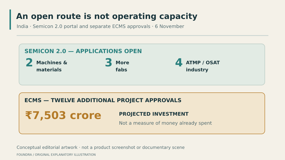
The Ministry of Electronics and IT’s release describes six Semicon 2.0 pillars: chip design; machines and materials; more fabs; strengthening the ATMP/OSAT industry; research and development; and talent. The newly launched portal accepts applications for pillars 2, 3 and 4. It is not an announcement that applications under all six pillars have opened.
For founders, this is first a classification problem. A proposal concerning manufacturing equipment belongs to a different technical activity from designing a chip or training engineers. The relevant programme rules, rather than the breadth of the announcement, determine eligibility. No approval or financing entitlement follows merely from identifying an electronics-related idea.
The approval batch: components and inputs
The ECMS section of the government release is a different part of the news. Twelve additional applications have received approvals, covering ten target-segment products. The ministry groups them into four components, five supply-chain products, and capital goods and their parts. These projects should not be recast as twelve new semiconductor fabs.
The four component categories are multilayer printed circuit boards, relays, heat sinks and specialty ceramics. The five supply-chain products are copper foil, anode material, cathode active material, polypropylene film and camera rims. Capital goods complete the list. The range reaches from materials to finished components to the machinery used in manufacturing.
That range changes the way the batch should be read. An ecosystem does not become more capable through one product category alone. A component manufacturer can depend on materials, tooling and process equipment supplied by other firms. The approvals describe proposed additions at several points in that chain, rather than one uniform kind of production capacity.
Three states of a manufacturing opportunity
Application route
Semicon 2.0 applications are open for pillars 2, 3 and 4.
Project approval
Twelve additional ECMS approvals carry stated investment, production and job projections.
Operating evidence
Actual spending, qualification, output and filled jobs need later project-level verification.
Materials have their own customer logic
The release identifies first-time ECMS approvals for copper foil, cathode active material and specialty ceramics. It describes copper foil as an input for copper-clad laminates used in PCBs and for lithium-ion cells, and polypropylene film as a capacitor-grade dielectric film. Those descriptions show why a materials project can connect to more than one downstream electronics activity.
The commercial problem for a materials supplier is consequently not identical to selling a finished consumer device. A buyer has to incorporate the input into another manufacturing process. Product specifications, consistency and qualification become part of that relationship. This is industry analysis of the supply-chain roles described in the release, not a claim that the approved suppliers have already passed a particular customer’s tests.
For startup readers, the opportunity map is more precise when the material and its intended use are named. A general statement about an electronics boom says little about which engineering skill, process or customer problem could matter. The approved categories offer a more concrete vocabulary for examining those questions.
Capital goods are part of the same stack
The ministry’s capital-goods list includes precision moulds and tooling, power and control systems for capital equipment, and factory-automation equipment and system integration. Its named approvals include TDConnex, Rockwell Automation India and Wipro Pari Robotics for those respective activities. These are disclosed approval subjects, not new contracts awarded to unspecified startups.
Equipment and integration also deserve separate treatment from materials. Their value to a manufacturer depends on how they fit into a production system and the support needed to operate it. Treating every approved category as an interchangeable unit of “electronics capacity” would hide that distinction. A supply-chain account should keep the engineering function visible.
Put the figures beside the right scheme
For this twelve-application ECMS batch, the government gives ₹7,503 crore of projected investment, ₹39,045 crore of projected production and 7,127 expected direct jobs. Those are projections, not spending, output and filled positions already measured. They belong to the ECMS approvals, not to the act of opening the Semicon portal.
Read together, the announcement is a programme map: specified semiconductor applications can now be submitted, while a component-manufacturing scheme has approved a batch spanning materials, components and machinery. Keeping those categories and their figures attached to the right programme makes the news usable without pretending that all electronics manufacturing is the same business.
Sources
- PIB / Ministry of Electronics and IT — November 6 Semicon 2.0 and ECMS release ↗ PIB / Ministry of Electronics and IT — November 6 Semicon 2.0 and ECMS release · Primary source
- YourStory / PTI — electronics component approvals report ↗ YourStory / PTI — electronics component approvals report
Have additional information? Request a correction.